|
|
|
|
Safety_Critical_Machine_Learning |
|

|
Space radiation is one of the most important
issues to consider in the design of space systems. Electronic equipment that is
used in space missions and satellite devices encounters ionizing particles,
which can cause some problems in their normal operation. The damage caused by
cosmic radiation to electronic equipment can be divided into three
categories: total ionizing dose (TID), displacement damage (DD) and single
event effect (SEE). Some countermeasure systems must be incorporated
into the design of space systems in order to address radiation damage to
successfully execute a space mission. One of the most effective solutions is
the design of adequate shielding to protect sensitive electronic parts. Lightweight materials cannot efficiently attenuate
the energetic electrons and protons, and heavy materials can create secondary
particles. The combination of high-density shielding materials and
low-density shielding materials is an ideal strategy.
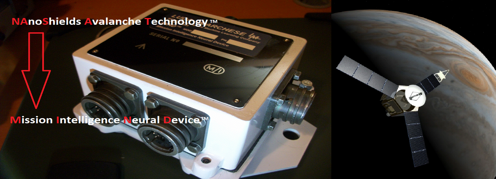
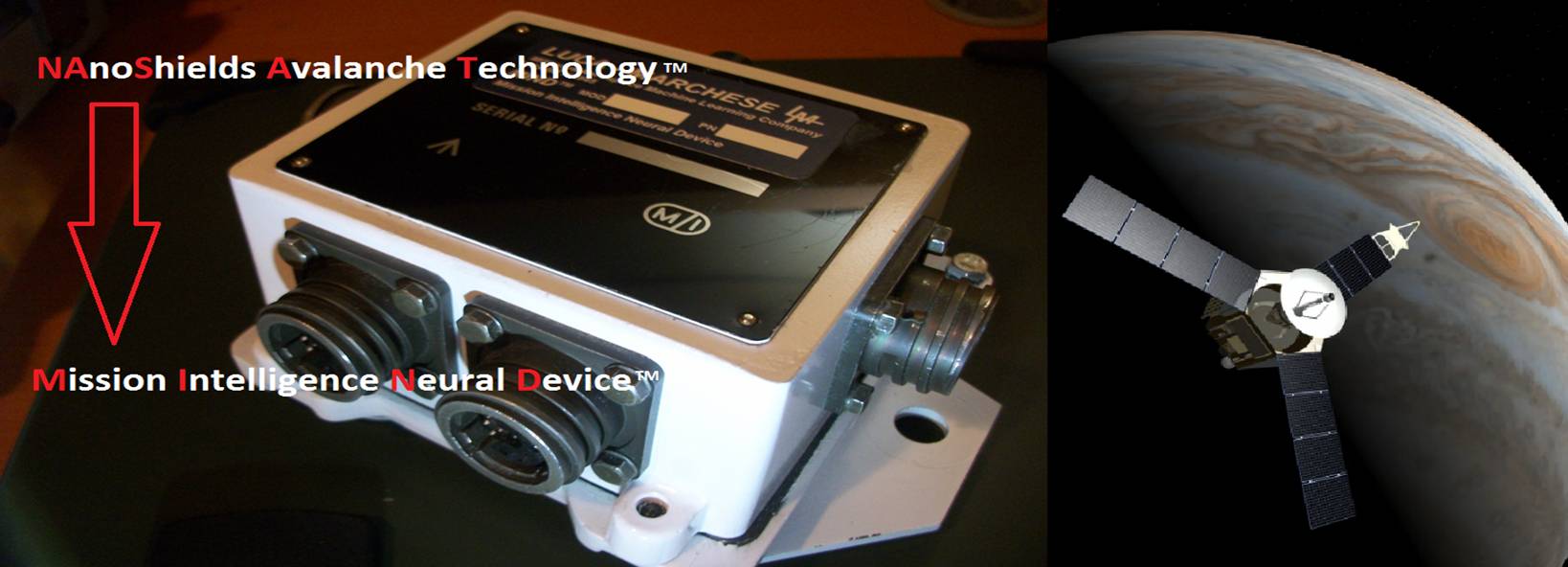
NASAT™ technology is based on a large sequence of HD and LD shielding nano-components. This nanotechnology based on Tungsten and Boron nano-components has been optimized through the use of
software simulators and genetic algorithms. The size of the nano-components, their distribution and proportion in the
epoxy suspension are characteristics of this technology for shielding gamma
and neutron radiation. Space is a very complicated environment and
contains a large variety of particles with different characteristics.
Actually, there is no laboratory practically to simulate such a complex
environment on the Earth. Therefore computational methods are effective tools
to design radiation shields. NASAT™ technology effectiveness has been
evaluated with computational methods based on simulation tools (e.g. Geant4)
and validated by experimental results with some limits. The performance of NASAT™ technology has been
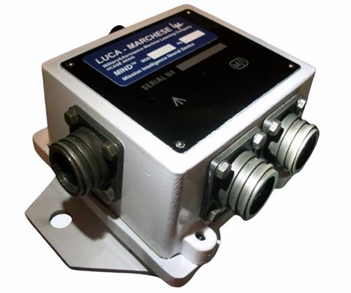
evaluated in the context of the geometrical properties of the MIND™ device. A
Genetic Algorithm has been used to process the results from simulations
(fitness-function of the GA) and optimize the density of nano-components. Another GA has been used to optimize the
geometrical disposition of electronic components. This optimization is
obtained by minimizing the incident radiations on the surface of the silicon
wafer for all the electronic devices or by maximizing the effectiveness of
Tripe Modular Redundancy relatively to all the possible positions of one
radiations source.
|

|
|
|
General Synaptics Aerospace_and_Defence_Machine_Learning_Company VAT NUMBER:_IT02670700992 REA NUMBER: GE-503104 Email:_luca.marchese@synaptics.org |
|
|
|
Copyright© 2026 General Synaptics |